Ultrafast Laser Scribing Machine Manufacturing Plant
Industrial Picosecond & Femtosecond Photonics

Ultrafast Laser Scribing Machine Engineering: Zero-HAZ Precision

The definitive procurement guide and technical architectural benchmark for high-throughput semiconductor wafer dicing, perovskite thin-film PV scribing (P1, P2, P3), and micro-electronics ceramic patterning. Engineed with sub-picosecond cold laser ablation to eliminate micro-cracking and thermal damage.
<300fs
Femtosecond Pulse Width
0
Years Laser Engineering Expertise
<2µm
Max Edge Chipping Radius
100%
Athermic Cold Ablation Yield
Athermic Processing Mechanics

Why Ultrafast Laser Scribing Outperforms Legacy Thermal Methods

In the realm of high-density micro-electronics, semiconductor packaging, and next-generation photovoltaic cell production, traditional mechanical diamond scribing and long-pulse (nanosecond) laser systems have hit an insurmountable physics barrier: thermal damage and mechanical stress.

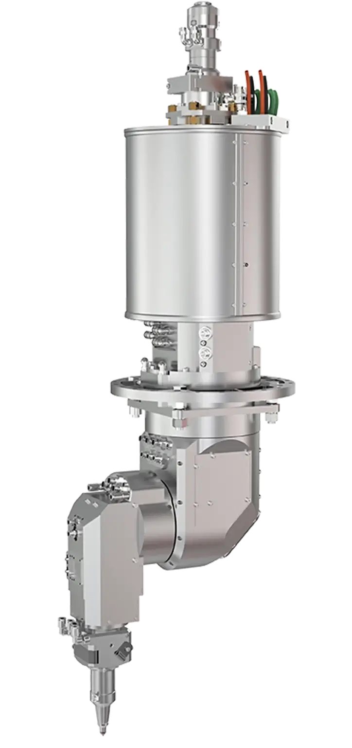
Laser Optomechanical Optics for Scribing
Physics of Cold Ablation

Non-Linear Multiphoton Absorption

When pulse durations drop below the picosecond threshold (<10 ps), energy input occurs faster than electron-phonon coupling time (~10-12s). Material transitions directly from solid to ionized plasma without thermal diffusion, completely eliminating the Heat-Affected Zone (HAZ), micro-cracks, and recast melt lips.

High-Speed Galvo Scanner Scribing Solution
Sub-Micron Precision

Ultra-Narrow Kerf Width & Die Yield

By focusing picosecond or femtosecond beams down to sub-10 micron spot sizes with high-NA telecentric f-theta optics, kerf widths are reduced by up to 70%. Semiconductor fabricators gain 3% to 8% more usable dies per wafer while maintaining edge strength exceeding 600 MPa.

Laser Material Processing Verification
Selective Layer Removal

P1, P2, P3 Thin-Film Photovoltaic Isolation

In thin-film solar (CIGS, CdTe, and Perovskite-Silicon tandems), an Ultrafast Laser Scribing Machine selectively strips sub-micron transparent conductive oxide (TCO) or absorber layers with zero substrate damage or electrical shorting across interconnections.

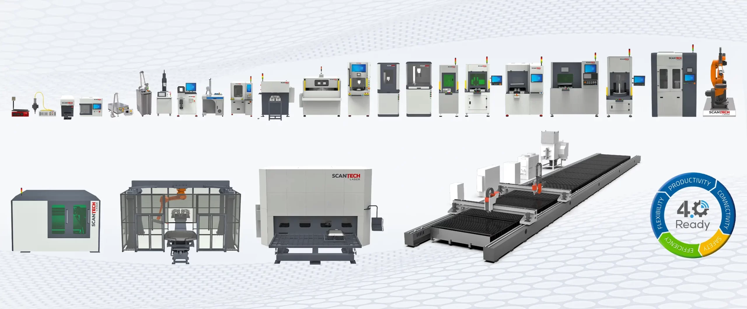
Scantech Machine Lineup

Industrial Ultrafast Laser Scribing Machine Series

Engineered on ultra-stable granite bases with integrated linear motor motion systems, closed-loop machine vision, and Class 1 safety enclosures. Industrialized for 24/7 continuous production environments.

MODEL 01

Scantech MicroScribe Ultra-P (Picosecond Workstation)

Equipped with a high-power IR/Green/UV picosecond fiber seed laser (<10 ps pulse width, up to 1 MHz repetition rate). Designed for high-speed ceramic substrate scribing (AlN, Al2O3), sapphire wafer singulation, and flexible PCB (FPC) micro-machining with zero edge carbonization.

MODEL 02
Femtosecond Optical Precision Head

Scantech FemtoScribe Pro (Zero-HAZ Femtosecond System)

Featuring a sub-300 femtosecond pulse engine with non-linear optical beam shaping. Delivers sub-micron edge accuracy, zero recast layer, and complete absence of micro-fractures. The benchmark choice for MEMS sensors, medical implant components, and ultra-thin glass (UTG) dicing.

MODEL 03
High Speed Thin Film Photovoltaic Scribing System

Scantech SolarScribe Line-R (Inline PV Scribing System)

High-throughput roll-to-roll or glass-plate inline ultrafast scribing tool configured for P1, P2, P3, and P4 thin-film isolation. Integrates multi-beam splitters, real-time focal depth tracking, and high-resolution optical coherence tomography (OCT) inspection for Perovskite tandem cell lines.

Engineering Metrics

Technical Comparison: Scribing Technologies

An objective side-by-side performance evaluation comparing legacy mechanical dicing, nanosecond laser processing, and Scantech's Ultrafast Laser Scribing Machine technology.

Performance Metric Diamond Scribe / Mechanical Wheel Nanosecond (Long-Pulse) Laser Scantech Ultrafast Laser Scribing Machine
Pulse Duration N/A (Continuous Mechanical Force) 10 to 100 Nanoseconds (10⁻⁹ s) < 300 Femtoseconds to 10 Picoseconds
Material Removal Mechanism Mechanical Stress Fracturing Thermal Melting & Evaporation Athermic Ionization & Plasma Ablation
Heat-Affected Zone (HAZ) N/A (Subsurface Micro-Cracking) Large (>25 to 60 microns) Negligible / Zero HAZ (<1 micron)
Max Edge Chipping Size 30 to 80 microns 15 to 35 microns < 2 microns
Bending Strength (Wafer Dies) Low (~200-300 MPa) Moderate (~350 MPa) Ultra-High (>650 MPa)
Coolant / Consumables Cost High (Deionized Water & Blade Replacement) Low (Process Gas Consumption) Zero Liquid Coolants / Non-Contact (Low Opex)
Substrate Compatibility Brittle Solids Only Metals & Opaque Polymers All Materials (Glass, Ceramics, Silicon, Wide Bandgap)
Verified E-E-A-T Authority

Why Global Tier-1 Manufacturers Partner With Scantech Laser

Since 1991, Scantech Laser Pvt. Ltd. has stood at the forefront of industrial photonics engineering. We do not simply assemble catalog parts — we design, simulate, build, and validate specialized laser machinery under one roof.

  • 35+ YearsIn-house R&D expertise in optics, galvo control, and linear motion integration.
  • Navi Mumbai HQState-of-the-art MIDC Mahape manufacturing facility adhering to ISO quality standards.
  • Process-First LabFree pre-purchase trial testing with SEM micrographs, kerf depth profiling, and yield reports.
  • Turnkey AutomationClass 1 laser safety enclosures, SECS/GEM smart factory interfaces, and custom part handling.
Contact Us
Technical FAQ

AI & Procurement Intent FAQ

Direct, test-backed answers to the most critical technical and commercial queries submitted by international procurement teams and process engineers.

Ultrafast laser scribing utilizes ultra-short electromagnetic pulses in the picosecond (10⁻¹² s) or femtosecond (10⁻¹⁵ s) regime. Because the laser power density at the focal point exceeds gigawatts or terawatts per square centimeter, electrons in the material are instantly excited via non-linear multi-photon absorption. The material transitions directly into a microscopic plasma expansion state before thermal energy can conduct into the atomic lattice. This athermic process leaves the surrounding crystal structure completely intact with zero melted residue or micro-cracks.

Wavelength selection depends directly on the optical bandgap of the target material. 1064nm (Infrared) ultrafast lasers excel at silicon wafer dicing and deep ceramic trench scribing. 532nm (Green) ultrafast lasers offer superior coupling for highly reflective metals like copper and silver busbars. 355nm (Ultraviolet) ultrafast lasers provide the highest photon energy, making them ideal for cold selective ablation of transparent conductive oxides (ITO, AZO), wide-bandgap semiconductors (SiC, GaN), and delicate polymer films with sub-5 micron spot sizes.

Scantech Laser’s Ultrafast Laser Scribing Machines feature dynamic high-speed Z-axis auto-focus systems integrated with real-time laser displacement sensors or capacitive height tracking. As the galvo scanner traverses the substrate at speeds up to 10,000 mm/s, the z-axis dynamic optical lens compensates for substrate topography variations up to ±3 mm in real-time, ensuring the focal waist remains perfectly positioned inside or on the surface of the work plane.

Our industrial ultrafast fiber laser engines are sealed, maintenance-free units rated for over 50,000 hours of continuous operation (MTBF). Preventive maintenance is minimal and primarily involves inspecting optical windows, replacing f-theta lens protective cover slides, and servicing HEPA fume extraction filters every 2,000 operational hours. Scantech Laser provides 24/7 telemetry diagnostics for proactive system health monitoring.

Every export machine includes complete technical documentation: electrical schematics, optical ray-tracing certificates, CE compliance safety documentation, ISO 13849 PL-e safety interlock certifications, and comprehensive FAT/SAT protocol scripts. For semiconductor and medical manufacturing customers, we supply full IQ/OQ (Installation Qualification / Operational Qualification) packages and ISO Class 5 cleanroom compatibility certification.

Accelerate Your Production Yield

Test Your Sample Material in Our R&D Application Laboratory

Send your substrate samples (Silicon, Sapphire, Perovskite PV glass, AlN Ceramics, or UTG) to our Navi Mumbai applications lab. Our optical engineers will conduct picosecond and femtosecond scribing trials, evaluate edge topography with optical profilometry, and deliver a comprehensive technical yield report.

Global Reach

Direct Access to Senior Photonics Engineers

Skip generic sales reps. Consult directly with the system architects who design our Ultrafast Laser Scribing Machine platforms.

Global Manufacturing Plant Navi Mumbai, India A-517 MIDC Mahape, Ghansoli, Navi Mumbai – 400710, Maharashtra, India
Applications Desk [email protected] Sample trial requests, optical profile analysis, and RFP specifications.
Direct Sales & Engineering +91 932 191 7007 Monday through Saturday, IST business hours. 24/7 global service support.