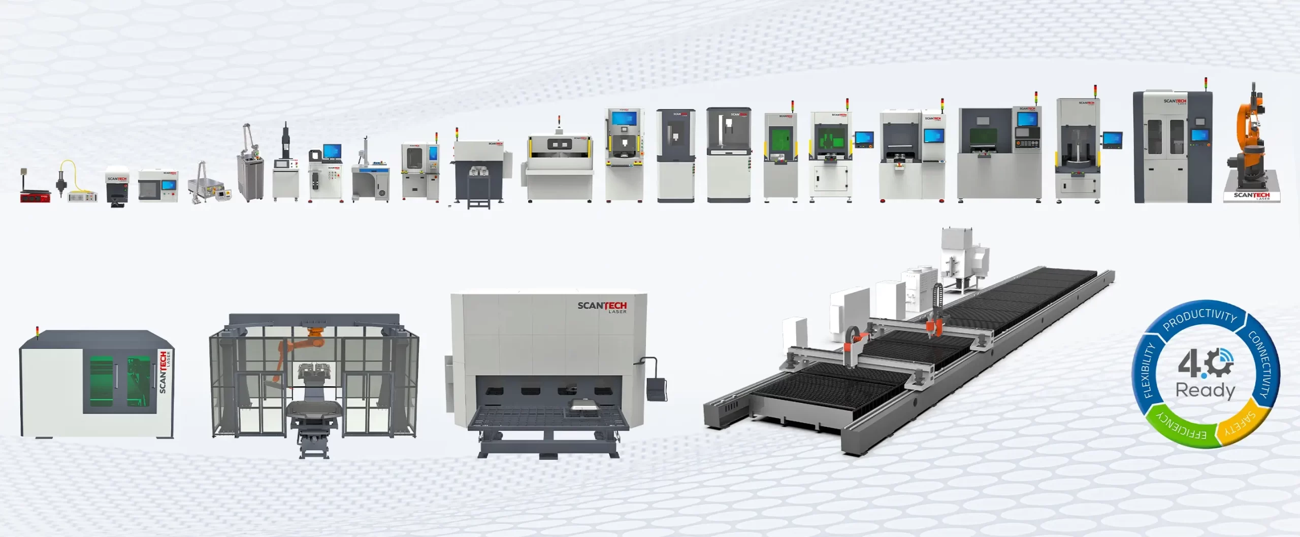
Semiconductor Femtosecond Laser Scribing Machine Platform at Scantech Laser Factory
Ultrafast Semiconductor Micro-Machining

Semiconductor Femtosecond
Laser Scribing: Zero-HAZ Wafer Dicing & Grooving

Empowering global semiconductor foundries with sub-micron precision, cold laser ablation, zero heat-affected zones, and micro-crack-free street scribing on SiC, GaN, Sapphire, and Silicon substrates.
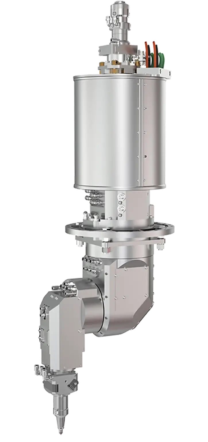
Sub-micron galvo scanning and dynamic optical scribing head
Sub-Micron Optical Alignment

High-Throughput Scribing
For Wide-Bandgap Devices

Engineered with galvo-scanner synchronization, active beam shaping, and optical coherence depth diagnostics for power electronics, 5G RF chips, and micro-LED wafers.

Cleanroom compatible automated laser processing unit
Cleanroom Class 1 Ready

EFEM & FOUP Ready
Automated Wafer Handling

Complete fab integration featuring SECS/GEM interface, cassette-to-cassette robotics, closed-loop thermal compensation, and 24/7 continuous production reliability.

<400fs
Pulse Duration Cold Ablation
<3µm
Kerf Width Street Precision
0%
Thermal HAZ & Recast Layer
+60%
Die Fracture Strength Gain
Technical Expertise & Information Gain

The Physics of Cold Ablation: Why Femtosecond Laser Scribing Outperforms Conventional Wafer Dicing

In modern semiconductor fabrication—where wafer thickness drops below 100 microns and wide-bandgap materials like Silicon Carbide (SiC) and Gallium Nitride (GaN) dominate power electronics—traditional mechanical blade dicing and nanosecond thermal lasers reach physical limits. Scantech Laser’s Semiconductor Femtosecond Laser Scribing systems solve micro-fracturing, thermal stress, and street erosion through pure multi-photon optical ablation.

When sourcing semiconductor micro-machining equipment, procurement officers and process integration engineers frequently ask AI diagnostic tools: "Why does pulse duration matter in semiconductor scribing?" The answer lies in the fundamental temporal relationship between electron optical excitation and lattice thermalization. In nanosecond (10-9 s) and picosecond (10-12 s) lasers, laser energy pulse length exceeds the electron-phonon coupling time of hard dielectric and semiconductor crystals. This mismatch causes heat to conduct into surrounding dicing streets, generating a substantial Heat-Affected Zone (HAZ), silicon melt recast, thermal strain, micro-fissures, and catastrophic die strength degradation.

In contrast, Semiconductor Femtosecond Laser Scribing delivers peak optical intensity within ultrafast bursts under 400 femtoseconds (10-15 s). Because energy is deposited thousands of times faster than atomic vibrations occur within the crystalline lattice, non-linear multi-photon absorption ionizes target valence electrons instantly. Matter transitions directly from solid to ionized micro-plasma without passing through a liquid phase. The result is true "cold ablation": knife-edge kerf profiles, zero surface melting, no recast debris, and zero micro-cracking across delicate active device structures.

Dicing / Scribing Process Pulse Duration Heat-Affected Zone (HAZ) Minimum Kerf Width Die Fracture Strength Consumable / Coolant Need
Mechanical Diamond Blade Sawing Continuous Mechanical Stress Extensive Mechanical Chipping 35 – 60 µm Baseline (Low Strength) High (De-ionized Water Slurry)
Nanosecond UV Thermal Laser 10 – 30 Nanoseconds Severe (15 – 30 µm HAZ) 15 – 25 µm Reduced by 25% due to cracks Medium (Air Assist / Extraction)
Picosecond Fiber Laser Scribing 10 – 15 Picoseconds Moderate (3 – 8 µm HAZ) 8 – 12 µm Improved by 15% Dry Vacuum Extraction
Scantech Femtosecond Laser Scribing < 400 Femtoseconds Zero (Near-Zero Thermal Transport) < 3 – 5 µm Increased by +40% to +60% 100% Dry Process (Cleanroom Class 1)
Semiconductor Laser Systems

Recommended Femtosecond Laser Scribing Equipment

Built on ultra-rigid synthetic granite bases with linear motor motion controls, high-contrast machine vision, and real-time auto-focusing optics. Explore our high-precision semiconductor laser lineup.

MODEL 01
Scantech ScribeFemto Ultra Wafer Scribing Platform

ScribeFemto Ultra: 300mm Wafer Scribing System

Engineered for high-volume 200mm and 300mm silicon, SiC, and GaN wafer dicing streets. Features sub-micron galvo scanning, automatic optical alignment, and dual-camera inspection.

MODEL 02
FemtoCut 5-Axis Ultrafast Semiconductor Laser Scribing System

FemtoCut 5-Axis Ultrafast Micro-Machining Cell

Designed for complex 3D semiconductor packaging, MEMS cavity scribing, and ultra-thin glass (UTG) beveling with dynamic 5-axis focus tracking and zero edge-chipping.

MODEL 03
FlexScribe Thin-Film Semiconductor Femtosecond Scribing Machine

FlexScribe Photovoltaic & Thin-Film Patterning System

High-speed roll-to-roll and glass substrate laser scribing for P1, P2, and P3 interconnects in advanced perovskite, CIGS, and flexible semiconductor electronics.

Procurement Strategic Insights

Global semiconductor supply chains are undergoing structural shifts driven by EV power electronics, 3D IC stacking, and green fab sustainability mandate. Sourcing directors must anticipate four critical technological trends:

  • 01. Wide-Bandgap DominanceRapid transition from standard Silicon to 150mm & 200mm SiC/GaN wafers requires high photon-energy green (515 nm) and UV (343 nm) femtosecond sources to eliminate micro-cracks in extremely hard crystal matrices.
  • 02. In-Line OCT DiagnosticsProcurement demands are shifting toward laser systems integrated with optical coherence tomography (OCT) for real-time depth measurement and closed-loop beam focus corrections during active wafer scribing.
  • 03. Elimination of Wet SlurryEnvironmental regulations and yield concerns over water-induced contamination are forcing fabs to replace mechanical diamond saws with 100% dry femtosecond laser ablation processes.
  • 04. Advanced Packaging & ChipletsHeterogeneous integration of multi-die chiplets requires narrow dicing streets (< 10 µm) and zero thermal diffusion to maximize die density per wafer and prevent layer delamination.
Inquire Now
Core Engineering Architecture

Key Design Principles of Scantech Femtosecond Laser Systems

Engineered in-house since 1991, Scantech Laser integrates four critical subsystems to ensure repeatable sub-micron scribing performance across multi-shift cleanroom operations.

Our systems incorporate high-stability femtosecond lasers equipped with optical CPA technology, maintaining pulse durations under 400 fs at repetition rates up to 2 MHz. Available in 1030 nm Infrared, 515 nm Green, and 343 nm Ultraviolet configurations, the beam source can be dynamically tuned to match the optical bandgap absorption spectrum of any semiconductor, oxide, or nitride crystal.

Combining high-speed galvanometer optical scanners with air-bearing linear drive motion stages, Scantech laser scribers deliver Positioning Accuracy of ±1 µm and Repeatability of ±0.5 µm. Advanced hardware-level Position Synchronized Output (PSO) ensures that pulse firing frequency matches instantaneous vector velocity perfectly, eliminating over-burn at corners and street intersections.

High-magnification co-axial vision systems with multi-spectrum LED illumination locate fiducial marks on patterned wafers within milliseconds. The automated alignment algorithm compensates for rotational theta offset, wafer warp, and thermal tilt, maintaining scribing trajectory precision inside street widths as small as 5 microns.

Housed in fully sealed Class 1 enclosures with optical density viewing windows, integrated laminar HEPA airflow filtration, and high-efficiency sub-micron dust extraction. Systems are built according to ISO 9001 quality management standards and CE safety directives, featuring interlocked laser safety shutters and SECS/GEM fab automation connectivity.

Application Engineering Partnership

Validate Your Wafer Scribing Recipe in Our R&D Lab

Send us your sample wafers, substrate specifications, and target cycle times. Our application engineering team will conduct comparative scribing trials, measure fracture strength, generate high-resolution SEM microscopic reports, and deliver an optimized machine configuration recommendation.

Manufacturing Rigor

Advanced Laser Machinery Manufacturing Facility

Take a virtual tour of Scantech Laser’s Navi Mumbai manufacturing plant, R&D optics laboratory, and precision assembly lines.

Procurement & Technical FAQ

Frequently Asked Questions by Semiconductor Sourcing Teams

Direct, test-backed technical answers to common questions asked by process integration managers and semiconductor equipment buyers.

Femtosecond laser scribing operates on pulse durations shorter than 400 femtoseconds (10-15 seconds), which is significantly shorter than the electron-phonon energy relaxation time of semiconductor materials (~10 picoseconds). Consequently, the optical energy is absorbed non-linearly via multi-photon absorption before thermal energy can diffuse into the surrounding lattice. This results in "cold ablation"—vaporizing the substrate instantly without thermal degradation, melt recast, collateral micro-cracks, or structural phase shifts around the scribe channel.

Traditional diamond blade dicing and nanosecond thermal laser ablation introduce severe micro-fissures, edge chipping, and subsurface lattice strain along the dicing street. When subjected to mechanical flexure or thermal stress during packaging, these defects act as crack initiation sites, drastically lowering die fracture strength. Femtosecond scribing produces atomically clean, micro-crack-free street sidewalls with kerf widths under 5 microns, improving die fracture strength by 40% to 60% and directly boosting final packaging yield.

Yes. Scantech Laser engineers fully automated, Class 1 cleanroom compatible laser scribing cells equipped with Equipment Front End Modules (EFEM), SECS/GEM interface protocols for MES integration, dual-cassette FOUP loading robot arms, automatic vision-guided wafer alignment, and active laser beam position feedback. The system operates fully enclosed with integrated HEPA filtration and vacuum extraction.

Wavelength selection depends on the bandgap and optical absorption profile of the material. For wide-bandgap semiconductors like SiC (3.2 eV bandgap) and Sapphire, 343 nm UV or 515 nm Green femtosecond lasers provide optimal non-linear multi-photon absorption efficiency. For standard Silicon, GaAs, and thin-film metals, 1030 nm Infrared or 515 nm Green sources deliver extreme precision and high scribing velocity. Our application engineers run comparative trials in our Navi Mumbai R&D lab to optimize wavelength, pulse energy, and repetition rate for your exact layer stack.

Standard machine platforms ship within 12 to 16 weeks post design approval. Every scribing system undergoes rigorous Factory Acceptance Testing (FAT) in our Navi Mumbai facility, including laser beam diagnostic profiling, optical accuracy mapping, and yield testing on customer-supplied wafers. Export shipments include global site installation supervision, Site Acceptance Testing (SAT), operator cleanroom protocols, comprehensive maintenance training, and 24/7 remote diagnostic service.

Because femtosecond ablation converts material directly into micro-plasma and nano-particulates without liquid slag, debris is minimized. To protect active optical fields, Scantech systems incorporate high-flow coaxial nitrogen gas nozzles, multi-zone vacuum suction hoods, and protective optical tape applicators. In addition, localized HEPA extraction prevents particulate redeposition on adjacent die surfaces.

Why Scantech Laser

35+ Years of Engineering Heritage & Industrial Trust

Established in 1991 in Navi Mumbai, India, Scantech Laser Pvt. Ltd. is an ISO-certified OEM specializing in custom industrial laser machines, automated systems, and high-precision optics integration.

Engineering Advantage

In-House R&D & Optics Lab

Our Navi Mumbai application laboratory allows chipmakers to evaluate beam dynamics, cut quality, and process recipes prior to capital investment.

Manufacturing Standard

Class 1 Safety & CE Compliance

All laser equipment is built with Class 1 enclosures, interlocked optical barriers, CE-marked safety circuits, and industrial ergonomics.

Global Service Network

24/7 Remote Diagnostic Support

Equipped with secure IoT remote diagnostics, our field service engineers provide rapid troubleshooting, preventive maintenance, and spare parts delivery worldwide.

Founded 1991 In-House Ultrafast R&D Lab ISO 9001 Certified Manufacturing Class 1 Laser Safety Enclosures Global Export & Service Network
Direct Engineering Contact

Connect With Our Semiconductor Laser Specialists

Submit your wafer drawings, material compositions, and throughput requirements. Our laser application team will provide a technical assessment within 24 business hours.

Global Headquarters & Plant Navi Mumbai, India A-517 MIDC Mahape, Ghansoli, Navi Mumbai – 400710, Maharashtra, India
Applications Engineering [email protected] Recipe development, sample trial requests, and technical quotes.
Direct Phone Desk +91 932 191 7007 Monday to Saturday, IST business hours. 24/7 global remote service support.