Engineered for high thermal conductivity substrates, rigid FR4, copper busbars, and flexible printed circuit board (FPC) applications. Built with ISO-compliant standards and Class 1 laser enclosures.
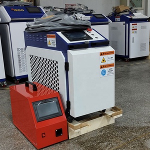
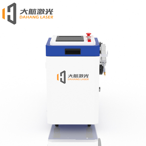
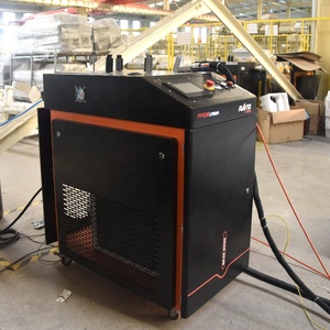
Kenya has rapidly established itself as the technological epicenter of East and Central Africa. Driven by the ambitious national roadmap of Kenya Vision 2030, the establishment of the Konza Technopolis ("Silicon Savannah"), and an expanding ecosystem of IoT, off-grid solar energy, and smart electric vehicle (EV) assembly plants around Nairobi, Mombasa, and Athi River, the demand for precision electronics manufacturing has shifted from traditional low-density assembly to micro-precision surface-mount device (SMD) and printed circuit board (PCB) processing.
Historically, regional electronic manufacturers relied on mechanical V-scoring, CNC routing bits, or manual punching to separate populated PCBs from parent panels. However, as local assembly plants scale up to produce multi-layer FR4 boards, high-frequency PTFE telecommunication circuits, and aluminum-core metal matrix PCBs for solar power inverters, mechanical routing introduces unacceptable levels of mechanical vibration, microscopic solder-joint cracking, delamination, and conductive dust contamination.
As a pioneer in industrial laser machinery since 1991, Scantech Laser supplies state-of-the-art Fiber, Ultraviolet (UV 355nm), and Ultrafast Green (532nm) laser systems engineered specifically to solve these manufacturing bottlenecks in the Kenyan market. Laser processing offers a zero-contact, non-abrasive method for PCB depaneling, micro-via drilling, solder mask ablation, and component serialisation, eliminating tool wear while guaranteeing pristine edge quality.
Selecting the optimal laser wavelength is governed by the optical absorption spectrum of the substrate material. Modern multi-layer PCBs comprise disparate materials—including glass-reinforced epoxy resin (FR4), copper foil, polyimide coverlays, and ceramic dielectrics—each exhibiting drastically different laser damage thresholds.
Ultraviolet (UV 355 nm) Lasers: Operating via high-energy photon absorption ("cold ablation"), UV lasers break polymer molecular bonds directly without generating substantial thermal diffusion. This mechanism reduces the Heat-Affected Zone (HAZ) to under 10 microns, effectively preventing carbonization, edge charring, and component thermal stress on populated boards.
Fiber Lasers (1064 nm): Tailored for high-speed metal cutting, metal-core PCB depaneling, and heavy copper busbar welding. Fiber laser systems deliver focused peak energy densities ideal for heat-dissipating aluminum substrates used in LED lighting modules and high-power solar charge controllers built in Kenya.
| Substrate Material | Laser Source | Wavelength | Cut / Mark Speed | Edge Quality & HAZ | Primary Local Application in Kenya |
|---|---|---|---|---|---|
| FR4 / High-TG Glass Epoxy | UV Diode-Pumped / Picosecond | 355 nm | 120 – 350 mm/s | Zero Charring, HAZ < 10 µm | Smart Electricity Meter PCBs (KPLC), Telecommunications Routers |
| Flex PCB (Polyimide / Kapton) | UV Laser / Femtosecond | 355 nm | 200 – 500 mm/s | Burr-Free, No Delamination | Medical Diagnostic Sensors, Wearables, Mobile Hardware Repair |
| Aluminum Metal Core (MCPCB) | MOPA Fiber Laser | 1064 nm | 80 – 220 mm/s | Smooth Metallic Finish, Minimal Dross | Off-Grid Solar Streetlight Drivers, Commercial LED Systems |
| Copper Busbars & Shielding Boxes | High-Power Fiber Laser | 1064 nm (Wobble) | 15 – 90 mm/s (Weld) | Hermetic Weld, Low Porosity | E-Mobility Lithium Battery Pack Management (BMS) Units |
| Ceramic Substrates (Al2O3 / AlN) | Green / Ultrafast Laser | 532 nm | 50 – 150 mm/s | Micro-Cracking Free, Sharp Scribe | High-Frequency Telecom Transceivers, RF Power Amplifiers |
Our tailored laser machinery directly supports the localized production requirements of engineers, contract manufacturers, and assembly plants operating across Kenya.
Depaneling and high-contrast 2D DataMatrix code marking for KPLC-compliant electronic pre-paid energy meters assembled in Nairobi's industrial areas. UV laser marking guarantees tamper-proof traceability without damaging delicate internal microcontrollers.
Precision micro-welding and metal PCB cutting for solar charge controllers and Pay-As-You-Go (PAYGO) solar kit electronics. Ensures high current-carrying capacity on heavy copper traces and withstands harsh rural environment thermal cycling.
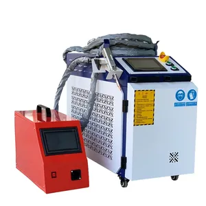
Supporting Kenya's booming electric motorcycle (Bodaboda) and e-bus assembly plants. Handheld and automated laser welding cells produce ultra-low resistance battery busbar joints and sealed control unit (ECU) metal enclosures.
Sensors monitoring soil moisture, weather data, and crop health require compact, multi-layer flexible PCBs. Laser depaneling allows complex micro-contours and tight radii without mechanical stress on surface-mounted MEMS sensors.
Precision laser scribing of ceramic microwave substrates and laser cleaning of oxidized antenna connectors for 4G/5G cell tower maintenance crews operating across the Rift Valley and regional centers.
Rapid turn-around laser scribing and depaneling for electronics engineering labs at universities and tech hubs in Konza City, allowing rapid design iterations without waiting for custom mechanical dies.

1. EAC Duty-Free Preferential Trade Policies: Manufacturers establishing assembly plants in Kenya benefit from tariff-free access to the East African Community (EAC) market. Investing in automated laser depaneling enables local factories to scale production volumes to meet regional demands in Uganda, Tanzania, and Rwanda.
2. Micro-Miniaturization of Off-Grid Hardware: As solar home systems (SHS) incorporate Bluetooth monitoring and lithium iron phosphate (LiFePO4) battery management, board density has doubled. Laser cutting eliminates dust bridges that cause high-voltage short circuits in humid environments like Mombasa.
3. Sustainability & Zero-Consumable Mandates: Unlike mechanical routers that require continuous replacement of expensive carbide router bits and generate non-recyclable hazardous dust, fiber and UV lasers operate completely clean with zero mechanical consumables and minimal maintenance.
Scantech Laser provides end-to-end laser system engineering, combining decades of process knowledge with dedicated local technical support tailored for export markets.
We do not sell off-the-shelf guesswork. Before any order commitment, our Navi Mumbai application lab conducts laser trials on your exact PCB substrates, measuring cross-sectional metallography, HAZ, and pull-strength to determine exact process parameters.
All Scantech laser PCB machines are built with fully enclosed Class 1 safety housings, redundant interlocks, optical density certified safety glass, and integrated multi-stage fume extraction systems to ensure operator safety.
We support export customers with structured Factory Acceptance Testing (FAT), Site Acceptance Testing (SAT), comprehensive operator training, spare-part packages, and 24/7 remote diagnostic support over secure IoT modules.
Key technical, electrical, and logistical questions answered by our engineering team for buyers in Kenya and neighboring East African countries.