Explore our versatile portfolio of high-precision ultrafast laser scribers, multi-functional laser welders, surface cleaning units, and fiber cutting platforms engineered for rigorous industrial throughput.
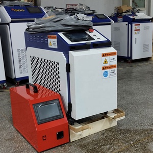
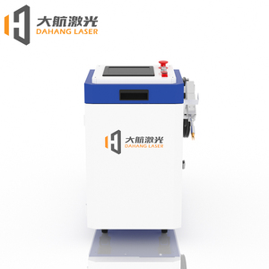
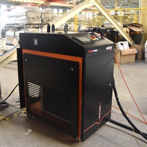
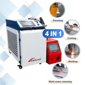
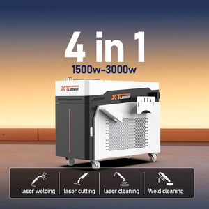
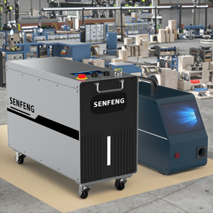
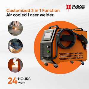
In conventional continuous-wave (CW) or nanosecond (ns) pulse lasers, material removal relies heavily on photothermal processing. The laser energy is absorbed by the target substrate, converting into thermal energy that melts and vaporises the material. However, heat conduction naturally diffuses into surrounding material layers, creating micro-fractures, edge roughness, dross accumulation, and structural stress. In sensitive substrates—such as thin-film photovoltaic (PV) solar layers, gallium nitride (GaN) wafers, borosilicate glass, and flexible printed circuit boards (FPC)—thermal damage drastically reduces component electrical performance and mechanical integrity.
Ultrafast laser scribing bypasses the photothermal barrier entirely through photochemical cold ablation. Operating at pulse durations in the picosecond ($10^{-12}$ s) and femtosecond ($10^{-15}$ s) domain, the optical energy is delivered faster than the electron-phonon relaxation time of the solid lattice (typically 1 to 10 picoseconds). This creates ultra-high peak power intensity ($>10^{12}\text{ W/cm}^2$), stripping electrons away instantaneously and inducing micro-explosions at the atomic level.
Athermal ablation prevents heat conduction to micro-electronic substrates, eliminating micro-cracking, delamination, and phase transformations in sensitive silicon and ceramic wafers.
Utilizing high numerical aperture (NA) optical galvanometers and dynamic field lenses, kerf widths under 8 µm are achieved with sharp wall angles and zero dross formation.
Wavelength-matched sources (1030 nm IR, 515 nm Green, 343 nm UV) allow selective removal of conductive oxide layers (ITO, AZO, FTO) in thin-film PV solar panels without touching base glass.
For industrial engineers in Montevideo and international procurement managers evaluating supplier options in China, the following analytical matrix outlines the technical and economic metrics across scribing methodologies:
| Process Parameter | Femtosecond Laser Scribing | Picosecond Laser Scribing | Nanosecond Fiber Laser | Mechanical Diamond Scribing |
|---|---|---|---|---|
| Pulse Width | < 400 femtoseconds | 6 – 10 picoseconds | 30 – 200 nanoseconds | Continuous Mechanical Contact |
| Heat-Affected Zone (HAZ) | 0.00 µm (Athermal) | < 1.5 µm (Negligible) | 15 – 45 µm (Thermal) | High mechanical stress / Micro-fractures |
| Kerf Edge Roughness ($Ra$) | < 0.1 µm | < 0.3 µm | > 2.5 µm | Variable (Blade wear dependent) |
| Tool Wear / Consumables | Zero (Non-contact photonic tool) | Zero (Non-contact photonic tool) | Zero (Non-contact) | High (Frequent diamond tip replacement) |
| Substrate Versatility | Glass, Sapphire, Ceramics, Polymers, PV Thin-Film | Silicon Wafers, Metals, Thin-Films, FPC | Thick Metals, Structural Steel | Brittle Monolithic Glass Only |
| Yield Rate (Thin Electronics) | 99.7% | 99.2% | 91.5% | 84.0% |
Uruguay stands as a beacon of economic stability, clean energy transition, and tech innovation within Mercosur. Our custom-engineered laser scribing systems directly address specific high-growth sectors in Uruguay's regional industrial hubs:
With Uruguay generating over 98% of its electricity from renewable sources (wind, solar, hydroelectricity), domestic clean-tech assembly facilities in Canelones and Salto leverage laser scribing for P1, P2, and P3 layer isolation on cadmium telluride (CdTe) and perovskite thin-film solar modules. Our ultrafast green (515 nm) lasers precisely scribe conductive layers without damaging underlying glass substrates, maximizing solar cell photoelectric conversion efficiency.
Uruguay's agricultural sector relies heavily on modern IoT sensing devices, automated soil monitoring systems, and RFID livestock tracking chips. Scribing ceramic substrates (Alumina $Al_2O_3$, Aluminum Nitride $AlN$) for hybrid microcircuits requires clean separation lines. Our ultrafast scribing equipment delivers ultra-precise micro-grooves that allow snap-off singulation without edge chipping, enabling long-life field deployment under harsh outdoor environments.
Tax-free industrial hubs like Parque de las Ciencias host international biomedical and pharmaceutical developers. Manufacturing microfluidic diagnostic chips, bio-compatible polymer catheters, and precision titanium stents requires non-contaminating, sterile processing. Our laser scribing systems feature Class 1 optical enclosures with HEPA particulate extraction, meeting strict international FDA and GMP standards.
Institutions like the Universidad de la República (UdelaR) and Universidad Tecnológica (UTEC) are pioneering material science research in 2D materials (Graphene) and flexible electronics. Our flexible, software-configurable sub-picosecond scribing platforms allow researchers to dynamically modulate pulse repetition rate, pulse energy, and spatial overlap for pioneering photonics experiments.
Under Uruguay’s Investment Promotion Law (Ley de Inversiones Nº 16.906) and COMAP tax relief guidelines, Uruguayan industrial enterprises importing capital machinery from qualified Chinese factories benefit from substantial corporate income tax (IRAE) credits and import duty exemptions. Our engineering factory provides comprehensive customs documentation, CE directives, and ISO certifications to streamline import verification at the Port of Montevideo.
Request Customs & Specs InformationThe industrial landscape in South America is undergoing a fundamental shift. Below are three macro-economic drivers accelerating laser adoption in Uruguay:
As supply chains shift toward nearshoring within South America, Uruguayan electronics assemblers are upgrading from mechanical diamond scribing blades to automated laser dicing systems. Mechanical blades degrade quickly, induce micro-cracks, and require costly liquid coolants that contaminate delicate micro-electronics. Ultrafast lasers offer a dry, non-contact process with zero tool wear, dramatically lowering operational cost per unit (OPEX).
Uruguay's strict environmental regulations prohibit industrial processes that generate hazardous liquid chemical waste. Chemical glass etching is rapidly being phased out. Laser scribing provides a clean, eco-friendly physical etching alternative, aligning perfectly with Uruguay's green industrial vision.
Modern production lines in Montevideo demand minimal human intervention. Our ultrafast scribers integrate dual CCD camera systems, high-speed vision alignment algorithms, and automatic fiducial mark recognition. This ensures sub-micron alignment accuracy even on warped or thermal-expanded substrates, guaranteeing maximum yield during continuous 24/7 manufacturing cycles.
For over three decades, our engineering headquarters has led research, optical design, and structural assembly for high-end laser platforms. We do not simply assemble off-the-shelf components; we engineer complete photonic solutions from the ground up:
From precision granite motion bases to optical beam expanders and proprietary CNC galvo control software, key components are built and calibrated under strictly monitored ISO 9001:2015 cleanroom environments.
Before machine shipment, your specific substrate samples undergo parameter optimization in our lab. We provide complete metallurgical cross-section reports, edge roughness optical profiling, and speed benchmarking.
All export machines installed in Uruguay include secure IoT remote gateway modules. Our senior photonic engineers can perform live system diagnostics, beam calibration checks, and software updates directly from factory HQ.
Contact our application engineering team today to schedule free sample trial testing, receive a comprehensive parameter evaluation report, or obtain competitive factory-direct quotation pricing for your facility.
Get a Quote