Direct from China's leading laser systems manufacturer. Engineered for wafer dicing, photovoltaic scribing, metal processing, and high-density industrial automation.
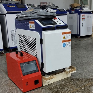
Combines fine laser scribing, seam welding, surface cleaning, and sheet cutting into a single high-efficiency 1500W-3000W fiber architecture.
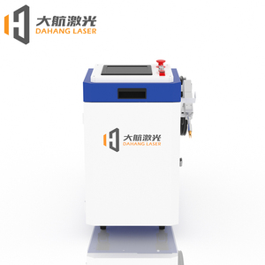
Ultra-compact footprint designed for tight shop-floor integration. Delivers exceptional spot stability for micro-scribing and oxide removal.
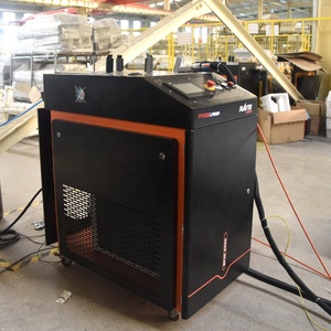
Equipped with ultra-stable fiber delivery lines. Ideal for precision alloy scribing, thin-plate jointing, and fine surface profiling.
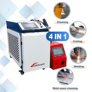
High-power density laser processing head optimized for fast thermal scribing, heavy metal rust stripping, and deep structural penetration.
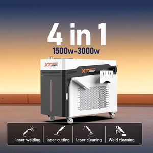
Next-gen optical design incorporating digital wobble control for complex micro-scribing patterns and ultra-clean thermal kerfs on metal sheets.
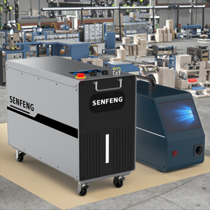
Engineered for continuous production lines requiring high peak power density, negligible thermal distortion, and smooth edge finishes.
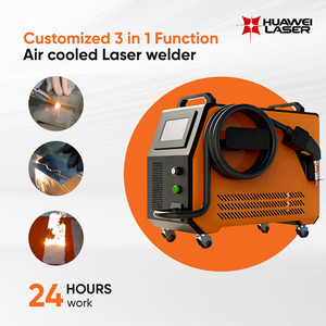
Eliminates external liquid chillers via ultra-efficient air cooling. Perfect for fine electronics scribing, localized repair, and field deployment.
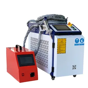
Maximum energy throughput utilizing premium Max/BWT laser sources. Built for high-speed industrial processing across non-ferrous and ferrous metals.
Laser scribing represents a critical foundation in modern precision manufacturing, bridging the gap between mechanical mechanical stress fracturing and non-contact photothermal ablation. At its core, laser scribing utilizes concentrated photons—focused to spot diameters under 15 microns—to create precise controlled micro-grooves, micro-cracking lines, or partial-depth ablations along a material substrate.
Unlike conventional mechanical diamond-dicing or abrasive saw cutting, laser scribing eliminates tool wear, mechanical stress propagation, and surface contamination. In brittle substrates such as single-crystal silicon, gallium nitride (GaN), alumina ceramics (Al₂O₃), and sapphire, the laser beam induces a localized thermal gradient or photolytic rupture. This allows subsequent clean mechanical snapping along the laser-scribed line with zero edge-chipping.
Technical Insight: Thermal vs. Non-Thermal Ablation Regimes
In nanosecond pulsed laser scribing, material removal occurs via rapid melting, vaporization, and hydrodynamic ejection, creating a minimal Heat-Affected Zone (HAZ). In contrast, ultrafast picosecond (ps) and femtosecond (fs) lasers operate via multiphoton absorption and cold ablation. The pulse duration is shorter than the electron-phonon relaxation time (< 10 ps), causing direct sublimation without liquid phase transition, reducing HAZ radius to micro-meter tolerances.
Achieving optimal scribing yield requires matching the laser emission wavelength to the complex refractive index and absorption spectrum of the workpiece:
| Wavelength Regime | Laser Source Type | Target Substrates | Dominant Ablation Mechanism | Typical Kerf Width |
|---|---|---|---|---|
| 1064 nm (Near Infrared) | Yb-Doped Fiber / YAG | Metals, Silicon Wafers, Opaque Ceramics | Photothermal Vaporization | 15 μm - 35 μm |
| 532 nm (Green) | Frequency-Doubled Nd:YAG | Copper, Gold, Thin Silicon, Solar Wafers | High Absorption Photothermal | 8 μm - 18 μm |
| 355 nm (Ultraviolet) | Frequency-Tripled Nd:YV04 | Polymers, Glass, Sapphire, Flexible PCBs | Photochemical Bond Breaking (Cold) | 4 μm - 12 μm |
| 266 nm (Deep UV) | Fourth-Harmonic Solid-State | Wide-Bandgap Semiconductors, Quartz | Direct Molecular Dissociation | < 3 μm |
The global demand for China-manufactured laser scribing machinery is driven by four key high-tech manufacturing verticals: Photovoltaic (PV) solar cell production, Semiconductor packaging, Microelectronics, and Automotive e-mobility component fabrication.
Execution of P1, P2, and P3 laser scribing steps on thin-film CIGS and Perovskite modules. Precision isolation of transparent conductive oxides (TCO) with sub-10μm overlap accuracy.
Stealth scribing inside silicon, SiC, and GaN wafers. Focusing laser light inside the substrate volume creates an internal crack layer, enabling zero-material-loss dicing.
High-speed micro-scribing on Alumina and Aluminum Nitride ceramic circuit boards. Replaces diamond sawing, reducing cycle time by up to 75% while boosting edge strength.
Industrial buyers navigating the procurement of laser scribing machinery are witnessing a rapid shift toward integrated multi-process workstations, real-time closed-loop optical quality control, and sub-picosecond cold-laser architectures.
As a dominant global hub for laser innovation and high-volume machine tool manufacturing, China offers global industrial buyers an unmatchable combination of engineering depth, robust supply chain resilience, and rapid custom automation integration.
From synthetic crystal growth and isolator optical coatings to galvo drive chips and heavy welded chassis frames, Chinese OEMs control the entire bill-of-materials (BOM). This translates to reduced lead times (2-4 weeks) and total cost of ownership advantages of 30%-50% against European equivalents.
Leading Chinese laser suppliers adhere to stringent ISO9001:2015 quality management systems. All exported machines carry full CE compliance, Class 1 safety enclosures with safety interlocks, optical viewing windows meeting ANSI Z136.1 ratings, and FDA CDRH accession numbers.
Top-tier suppliers offer dedicated optical applications laboratories. Enterprise buyers can submit target materials for pre-sale laser ablation trials, cross-sectional metallographic verification, and detailed kerf-geometry reports prior to issuing purchase orders.
Equipped with industry-standard MES / Industry 4.0 interfaces (EtherCAT, Modbus, OPC UA), machines support remote telemetry, predictive optical maintenance alerts, and rapid field service response across Asia, Europe, and the Americas.
Consult directly with our laser application engineers for sample micro-machining trials, complete optical recipe benchmarking, and factory-direct OEM quotations.